G.Skill Trident Z DDR4 module goes over 5000MHz

G.Skill Trident Z DDR4 module goes over 5000MHz

Toppc hits new memory frequency world record

G.Skill has announced that its Trident Z DDR4 memory has achieved a new frequency record of over 5000MHz.

The 4GB DDR4 Trident Z module was overclocked to a mind-boggling frequency of 2501.2MHz (5002.4MHz effective), under LN2, of course, and with MSI’s Z170I Gaming Pro AC motherboard and Intel Skylake Core i5-6600K CPU. The culprit is a well known Toppc overclocker and this score was enough to secure him the first place on HWBOT’s memory frequency list. The latency was set at 31-31-31-63 so it is obvious that the focus was on frequency and not the latency. It is also quite surprising that the overclocking was done on MSI’s mini-ITX motherboard..

The 5GHz frequency was a holy grail for quite some time and it does not come as a surprise thatG.Skill is quite proud that its modules were first to hit the magical mark. G.Skill’s Corporate Vice President and Director of R&D, Tequila Huang said that the company is “extremely excited to achieve this great milestone together with Samsung components and MSI motherboard” and that they “will continually push hardware performance to the limits and provide enthusiasts with even more advanced products.”

Previous memory frequency record on HWBOT.org of 2450.8MHz was held by Chi-Kui Lam on G.Skill’s Ripjaws 4 DDR4 module, so there is certainly a pattern here. Hopefully it won’t be long before we see DDR4 pushed even further.

Recently, G.Skill has announced its newest 16GB (8GBx2) high-performance DDR4-4266 Trident Z kit, so hopefully we wan’t wait too long for higher frequency records.

The validation screenshots can be seen below, while you can find more details at the HWBOT.org site or the CPU-Z validation page.

gskill tridentZ5ghztoppc 1

gskill tridentZ5ghztoppc 2


Via

MSI comes up with five GTX 1080 graphics cards

MSI comes up with five GTX 1080 graphics cards

Aero, Armor, Gaming X and Sea Hawk

MSI has unveiled a total of five different Geforce GTX 1080 graphics cards including a couple of rather interesting versions like the GTX 1080 Gaming X 8G with Twin Frozr VI cooler or the GTX 1080 Sea Hawk with Corsair’s Hydro Series hybrid cooler.

The list of MSI’s newly announced GTX 1080 graphics cards starts off with the GTX 1080 Founders Edition, which is all stock, and the the MSI GTX 1080 Aero graphics card which will also feature custom blower style cooler with s leek black and silver design. As most MSI graphics cards, the GTX 1080 Aero will also be available in two versions, one with reference 1607/1733MHz GPU clocks and the OC versions working at 1632/1771MHz clocks.

msi gtx1080lineup 1

The MSI GTX 1080 Armor uses MSI’ well known Twin Frozr V dual-fan cooler paired up with TORX fan technology and comes with a couple of MSI exclusive features like the Zero Frozr technology which does not spin up fans in idle. Unfortunately, it does not feature a backplate for some reason but does come with a factory-overclocked OC version working at 1657/1797MHz. MSI GTX 1080 Armor is also one of the GTX 1080 graphics cards in MSI lineup that features a custom PCB with 12-phase VRM which draws power from a 8- and 6-pin PCIe power connectors.

msi gtx1080lineup 2

The MSI GTX 1080 Sea Hawk is a hybrid cooled graphics card equipped with Corsair’s Hydro Series liquid cooler. The liquid cooler cools down the GPU while the blower fan cools down the VRM, memory and the rest of the board. According to what we see, MSI did not use a custom PCB on this one as it needs a single 8-pin PCIe power connector but the Corsair Hydro Series was enough to hit 1708/1847MHz clocks. The 8GB of GDDR5X memory on the Sea Hawk is also overclocked to 10108MHz.

msi gtx1080lineup 3

The flagship GTX 1080 in MSI’s lineup is the new GTX 1080 Gaming X graphics card which has three working modes and comes with MSI’s Twin Frozr VI dual fan cooler. According to details from MSI, the GTX 1080 Gaming X works at 1607/1733MHz in Silent Mode, 1683/1822MHz in Gaming mode and 1708/1847MHz in OC mode. The 8GB of GDDR5X memory is also overclocked to 10108MHz.

msi gtx1080lineup 4

According to MSI, the Twin Frozr VI should be significantly better than a reference cooler as it packs a huge heatsink, 8mm copper heatpipes, nickel-plater copper baseplate, premium thermal compound and new TORX 2.0 fans.

The MSI GTX 1080 Gaming X also comes with RGB LEDs on the side and a backplate.

MSI is one of the partners that has plenty of GTX 1080 graphics cards in its lineup and hopefully, custom ones will show up in retail/e-tail soon as currently, only Founders Editions are up for grabs.

msi gtx1080lineup 5

Via

Google makes major leap forward with new Tensor Processing Unit

Google makes major leap forward with new Tensor Processing Unit


Accelerator will move Moore’s Law forward by seven years

On Wednesday at Google’s annual I/O developer conference in Mountain View, California, the company went forward and announced a revolutionary new processing accelerator unit for machine learning that is now expected to move a recently-slowing Moore’s Law forward by at least three chip generations, or seven years.

venturebeat google tensor processing units

Image credit: VentureBeat.com

Google says its new Tensor Processing Unit, or TPU, is capable of delivering an order of magnitude higher performance-per-watt “than all commercially available GPUs and FPGAs.” The new accelerator unit is specifically built and custom designed for machine learning tasks. In fact, Google engineer Norm Jouppi says in a company blog post that the TPU accelerators have been running in company datacenters for more than a year, with at least one order of magnitude better performance-per-watt for machine learning tasks requiring reduced computational precision, such as deep learning and object recognition.

The name “Tensor Processing Unit” stems from the accelerator’s original application purpose –Tensor Flow, an open-source software library for computing very large mathematical datasets and interpreting them using visual graphs. The software was originally developed by Google’s Brain Team, a 12-month academic program specializing in machine learning, linguistics, data visualization and neural networks.

google ceo sundar pichai io 2016

Google CEO Sundar Pichai at I/O 2016 (via Yahoo Finance)

According to company CEO Sundar Pichai, the TPU accelerators will never replace CPUs and GPUs but they can speed up machine learning processes with a fraction of the power draw required by other ASICs. One drawback, however, is that ASICs such as Google’s TPU are traditionally designed for highly-specific workloads. In this case, the applications are TensorFlow and Cloud Machine Learning Alpha, which computes mathematical derivatives and other numerical datasets and allows more tolerance for reduced precision (see: half-precision FP16). Currently, only GPUs and newer CPUs (Intel Haswell and later) support half-precision calculations in TensorFlow. This processing mode is useful for deep learning by reducing memory usage of a neural network, delivers twice the performance of FP32, and allows training and deployment of larger networks over time.

google relative tpu performance per watt

Image credit: VentureBeat.com

“TPU is tailored to machine learning applications, allowing the chip to be more tolerant of reduced computational precision, which means it requires fewer transistors per operation. Because of this, we can squeeze more operations per second into the silicon, use more sophisticated and powerful machine learning models and apply these models more quickly, so users get more intelligent results more rapidly. A board with a TPU fits into a hard disk drive slot in our data center racks.”

Since the gradual slowing of Moore’s Law around mid-2012 (Intel’s last 2D planar architecture launch), scientists have been fervently attempting to defy the laws of atomic-level physics in order to justify the scalability of three-dimensional processor designs over the next two decades. While may claim that tri-gate CPU and FPGA designs will scale at the nanometer level for at least another seven years, Google is now claiming that its TPU will effectively bring 2023 performance-per-watt levels into the present for machine learning applications. The new accelerators will effectively skip three generations worth of Moore’s Law (roughly 2.5 years each), but they are little more than application-specific chips (ASICs) for “playing back” deep learning data. On the other hand, CPU and GPU clusters will still be required to discover and generate most underlying neural network algorithms by sifting through large, near-endless datasets.

Currently, Google uses TPUs to improve web search results using its RankBrain algorithm and to improve the overall accuracy and quality of Street View, maps and navigation routes in general. For now, however, Google senior vice president Urs Hölzle says the company doesn’t need to have TPUs inside every server rack just yet. The company has also ruled out the idea of making TPUs separately available for corporate and enterprise purchases.

According to Diane Greene, Google’s enterprise chief, one reason for this strategy has to do with the company’s cloud-centric business model. It would rather see its customers rent space for deep learning computations on its cloud-based machine learning datacenters (see: Cloud Machine Learning Alpha and pricing) – which require no front-end user maintenance while hardware upgrades (CPUs, GPUs and TPUs) are all performed on Google’s end by qualified engineering and IT staff. While this approach is arguably on the authoritarian side, it gives the company more leverage over some core cloud-focused business segments where research and development in deep learning are concerned. Consequentially, with the performance numbers Google announced today, we should expect some of the company’ competitors to offer deep learning ASICs in retail for consumer and enterprise use in the near future.

Via

EVGA officially launches the new X99 FTW K motherboard

EVGA officially launches the new X99 FTW K motherboard

E-ATX motherboard with the new 8-layer Hybrid Black PCB

After a couple of teasers, EVGA has now officially launched its new high-end motherboard based on Intel’s X99 Express chipset, the EVGA X99 FTW K.

Unveiled and teased earlier by both EVGA and Vince “K|NGP|N” Lucido, the new EVGA X99 FTW K motherboard is based on Intel’s X99 Express chipset with support for Intel’s upcoming Broadwell-E CPUs and it is an E-ATX form-factor motherboard. The X99 FTW K comes with a new all-black color scheme with a couple of red accents and uses the new 8-layer Hybrid Black PCB. The rest of the features includes a CPU socket with 150 percent higher gold content and an advanced 8-phase Digital VRM (IR3563B+IR3350).

The rest of the specifications include eight DDR4 memory slots with new 4-layer memory T-Routing system and support for up to 128GB of DDR4-3200+ memory, five PCI-Express 3.0 x16 slots and single PCI-Express x1 slot. Storage side includes 10 SATA 6Gbps ports and single M.2 slot and it also comes with two USB 3.1 (Type-A and Type-C) ports, Dual Gigabit Ethernet (Intel and Killer NIC), and 7.1-channel audio.

As this motherboard is a part of EVGA’s FTW lineup, it also comes with plenty of overclocking-friendly features including PCIe disable switches, dual BIOS, on-board power, reset and clear CMOS buttons, onboard CPU temp monitor and more.

The new EVGA X99 FTW K motherboard is already available directly from EVGA with a price of US $299.99.

evga X99FTWK 1

evga X99FTWK 2

evga X99FTWK 3


Via

Nvidia announces ultra high-resolution screenshot capture utility

Nvidia announces ultra high-resolution screenshot capture utility


Captures in-game screenshots at gigapixel resolutions with HDR

During its Geforce Pascal introduction on Friday, Nvidia CEO Jen-Hsun Huang introduced Ansel, the “world’s first in-game camera system” that enables two-dimension and three-dimensional screenshot capturing up to 32 times higher than in-game resolution – from megapixels to gigapixels with a completely adjustable field-of-view (FoV), among other features.

nvidia ansel user interface 700px

Nvidia Ansel user interface (Larger image here)

The software, named after American photographer and environmentalist Ansel Adams, will now allow gamers to capture in-game screenshots from infinite camera angles along with post-processing filters including High Dynamic Range (HDR) and traditional filters including “film grain,” “black and white,” sepia” and “hue shift.” The software also allows capturing screenshots in full 360-degree stereoscopic formats.

“Ansel is a revolutionary new way to capture in-game shots and view in 360. Compose your screenshots from any position, adjust them with post-process filters, capture HDR images in high-fidelity formats, and share them in 360 degrees using your mobile phone, PC, or VR headset.”

4K (8.3-megapixel) screenshots can now be saved in 8.3 gigapixel format

Once an in-game shot is framed and positioned by the user, it can then be saved in ultra-high gigapixel resolution by selecting the “High Resolution” option. This conveniently allows users to save images up to 1,000 times their current display resolution. With a 4K monitor (8.29 megapixels), for instance, an in-game screenshot can now be saved at a stunning 8.29 gigapixel resolution.

Duncan Harris, James Pollock , Leonardo Sang, Joshua Taylor and many other notable new media artists have created some galleries over the past few years with screenshots ranging from Street Fighter V, Mirror’s Edge, Gears of War, Star Wars Battlefront, Elder Scrolls V: Skyrim, Tom Clancy’s The Division, RAGE and Fallout 4 with emphasis on landscapes, portraiture, action sequences and other stylistic elements found in environmentally diverse in-game situations.

nvidia ansel super resolution

“Capture your shot in super resolution for the most detailed images and perfect edges. Capture up to an 8-Gigapixel image, or 32 times your game resolution.”

Ansel is also fully compatible with OpenEXR, a high dynamic range file format developed by Industrial Light and Magic for computer imaging applications.

“Show your creativity, your humor, your sense of style, and maybe even become the next professional game photographer, wowing the world with stunningly composed screenshots worthy of display in an art gallery and on enthusiasts’ walls,” NVIDIA writes. “Anything’s possible with Ansel, and it will all be available for GeForce GTX gamers.”

Nvidia has also launched an Ansel 360-degree image gallery featuring seven spherical 3D in-game screenshots that actually seem quite impressive. The company claims these dynamic screen captures can also be viewed on a VR headset and the images are compatible with any WebGL-enabled web browser.

The screen capturing software will initially be supported on a majority of midrange to high-end Nvidia Kepler, Maxwell and Pascal GPUs, beginning with Geforce GTX 650 all the way up to Geforce GTX 1080.

Available soon, compatible with a number of “top games”

ansel goming to games soon

The company claims that in-game support for the Ansel image capturing utility is “coming soon” and will include titles such as The Witcher 3, No Man’s Sky, Tom Clancy’s The Division, The Witnessand the Unreal Tournament series, among others.

Below are a few in-game creative pieces from some featured galleries by the aforementioned screenshot artists.

duncan harris the witcher 3 rockfall 700px

“Rockfall” from The Witcher 3 by Duncan Harris (Larger image here)

adr1ft walkabout series 029 duncan harris 700px

ADR1FT Walkabout Series 029 by Duncan Harris (Larger image here)

star wars battlefront pew pew by leonardo sang 700px

Star Wars Battlefront – “Pew Pew” by Leonardo Sang (Larger image here)

skyrim screenshot by james pollock 700px

Skyrim night screenshot by James Pollock (Larger image here)

leonardo sang corvega assembly plant fallout 4 700px

Corvega assembly plant in Fallout 4 by Leonardo Sang (Larger image here)

rage faces of the apocalypse by joshua taylor 700px

RAGE – “Faces of the Apocalypse” by Joshua Taylor (Larger image here)


Via

First AMD Zen chips may not be quad-core parts

First AMD Zen chips may not be quad-core parts


AMD prepares for IPC race with Intel

In May 2015, we reported that AMD’s first Zen CPUs, launching in Q4 2016, would most likely be quad-core chips based on a presentation slide showing the company’s Zen core units scaling up to four cores with shared L3 cache. According to new information released one year later, this may not be the case and, the company could be preparing to launch eight and six-core variants in a tight efficiency race against Intel’s ‘Kaby Lake’ CPUs.

amd zen based quad core unit 700px

AMD’s Zen-based quad-core unit slide from May 6, 2015. (Larger image here)

AMD’s official “Zen-based Quad Core Unit” slide” was released May 6, 2015 during its Financial Analyst Day when the company claimed its new platform will have a more competitively-focused IPC design, higher core counts, lower latency caches and will be based on second-generation 14nm Low-Power Plus (LPP) process technology.

amd zen roadmap

AMD’s Zen FX CPU roadmap slide from May 6, 2015. (Larger image here)

On Wednesday, sources close to the folks at Italian site Bitsandchips.it now suggest that AMD will produce 8-core and 6-core Zen x86 chips initially – and only in the event of bad yields will OEMs and ODMs decide to use quad-core variants. Due to the fact that Intel is launching 6-core and 10-core high-end Broadwell-E processors later this month, it appears AMD will be initially focused on bringing back some high-end desktop (HEDT) market share from Intel’s stagnant performance numbers.

In recent benchmarks, the Core i7 6950X is only about 10 percent faster than the Core i7 5960X in Cinebench multi-threaded performance, while the former Haswell-E chip is actually slightly faster in Cinebench single-threaded tests. This is a great place for AMD to gain some ground against Intel’s ‘Kaby Lake’ CPUs in Instructions Per Clock (IPC) by launching Zen with a higher number of cores, at least initially.

We mentioned in August 2015 that Zen uses SMT (hyperthreading) just like Intel’s cores and will be switching back to a single FPU-per core design. With this market approach, every core will be able to run two simultaneous threads just like Intel’s CPUs. This is AMD’s way of breaking from the “core pair” implementation that was established in Bulldozer in October 2011, also known as Clustered Multithreading (CMT).

Of course, AMD will eventually release a 16-core x86 Zen APU with Greenland integrated graphics, but this is not expected to compete with Intel until 2017 when 10-nanometer Cannonlake CPUs are released later in the year. AMD can also produce an 8-core and even 6-core version of this Zen APU

Bristol Ridge APUs will initially take dual-core and quad-core designs

Meanwhile, the company is planning to announce some new dual-core and quad-core APUs later this month at Computex 2016, codenamed Bristol Ridge, to compete with current Intel 6th-generation Skylake CPUs. These 7th-generation APUs are built using four ‘Bulldozer’ CPU cores and eight GPU cores, and AMD will categorize them as “entry level” CPUs when they launch later this summer. Already, HP has announced an Envy x360 15-inch convertible with dual-core and quad-core Bristol Ridge parts based on the AMD FX naming scheme.

GlobalFoundries has been ramping up production of its second-generation 14-nanometer technology, also known as 14 Low-Power Plus (14LPP) since Q4 2014 and provided some validation on production samples in December 2015. AMD has said in the past that it will not pay GlobalFoundries (or any foundry) to develop custom silicon for its architectural designs. With this in mind, the company is relying heavily on the success of the GF second-gen 14LPP process technology and fully-depleted silicon technology to restore its core PC business back to levels it has not experienced in years. The improvements should help AMD gain traction in both TDP efficiency and performance that will allow the company to effectively scale Zen designs across more market segments in years to come.

finfet soi vs bulk transistors
Fully depleted FinFET transistors (one fin shown here) — silicon-on-insulator vs. bulk silicon


Via

Alleged Nvidia Geforce GTX 1080 benchmarks spotted

Alleged Nvidia Geforce GTX 1080 benchmarks spotted

Scores higher than overclocked GTX 980 Ti 

Just a day ahead of the rumored May 6 event where Nvidia is expected to unveil its first Geforce graphics cards based on the Pascal architecture, alleged 3DMark benchmarks of the GTX 1080 have been spotted and it performance quite well.

There were already quite a few leaks regarding Nvidia’s upcoming GP104-based lineup, including the information that there will actually be three different SKUs, most likely named GTX 1080, GTX 1070 and GTX 1060 (Ti). While the GTX 1080 and GTX 1070 are expected to be unveiled tomorrow and probably available sometime later this month or early-June, the precise number of CUDA cores have not yet been confirmed.

According to the latest leak from Videocardz.com, the flagship Geforce GTX 1080 will actually come with 8GB of “new” GDDR5X memory clocked at 2,500MHz (10,000MHz effective) and paired up with a 256-bit memory interface. This will add up to a 320GB/s of memory bandwidth.

According to the leaked 3DMark benchmarks the Geforce GTX 1080 ends up with a 27,683 graphics score in the Performance preset and a 10,102 graphics score in the FireStrike Extreme benchmark. These are actually higher than what you would get from an overclocked GTX 980 Ti, which gets around 25,000 graphics points in Performance preset and around 8,700 in FireStrike Extreme preset.

With 16nm FinFET manufacturing process, the GP104 GPU is also expected to draw much less power compared to the 250W GM200 GPU on the GTX 980 Ti.

The Geforce GTX 1070 should be based on a cut-down version of the GP104 GPU, the GP104-200, and will probably end up with a lower number of CUDA cores and, according to the same leak, pack 8GB of GDDR5 memory, clocked at 2000MHz (8GHz effective). With the same 256-bit memory interface, the Geforce GTX 1070 will end up with a memory bandwidth of 256GB/s.

Of course, it is still too early to talk about the actual performance as we are sure that Nvidia will further tweak the driver performance but at least it gives us a clear picture on what to expect from Nvidia’s upcoming Geforce GTX 1080/1070 Pascal-based graphics cards.

Hopefully, Nvidia will reveal a bit more information at the rumored Pascal event scheduled for tomorrow.

Nvidia GTX10803dMarkperfleakVC 2

Via

Intel flagship Broadwell-E Core i7-6950X tested as well

Intel flagship Broadwell-E Core i7-6950X tested as well

Compared with the Core i7-5960X

It is obvious that Intel’s Broadwell-E HEDT launch is drawing near as with all the previous leaks we now have some of the first benchmarks of the flagship ten-core Core i7-6950X.

SiliconLottery user from the Overclock.net forums, which brought the first pictures and benchmarks of the octa-core Core i7-6850K, has managed to get its hands on the flagship Core i7-5960X as well, and compared it to the Haswell-E Core i7-5960X flagship CPU. Silicon Lottery is actually a store that has already placed the Core i7-6950X on pre-order with a price set at US $2,099.99.

Based on 14nm manufacturing process, the Broadwell-E Core i7-6950X CPU is a ten-core part with enabled Hyper Threading, which means that the OS will see a total of 20 threads. It works at 3.0GHz base and 3.5GHz maximum Turbo clocks, packs 25MB of L3 cache and has 40 Gen3 PCIe lanes. It supports DDR4-2400 memory and will be compatible with current Intel X99 Express chipset based motherboards, with BIOS update of course.

Intel Corei76950Xocn 4

Performance wise, the Core i7-6950X managed to get a Cinebench R15 score of 2327 points when overclocked to 4.5GHz. When pushed to 4.0GHz, it scored 1904 points, which is around 19.5 percent higher than the Core i7-5960X at the same clocks. Bear in mind that the new Broadwell-E Core i7-6950X actually has two more cores. The Core i7-6950X also offered higher memory write speed in AIDA64 benchmarks while the memory read speed was the same.

In a clock-to-clock comparison in Intel XTU Benchmark, the Core i7-6950X managed to get 2354 points, which was higher than 2001 for the Core i7-5960X.

Most motherboard manufacturers have already released their X99 motherboard BIOS updates in order to support the upcoming Broadwell-E CPUs so these benchmarks looks legit enough.

Intel is expected to launch its Broadwell-E HEDT (High-End Desktop) CPUs at Computex 2016 show which kicks off on May 31.

Intel Corei76950Xocn 1

Intel Corei76950Xocn 2

Intel Corei76950Xocn 3

Via

Nvidia begins Geforce Pascal with GTX 1080 and GTX 1070

Nvidia begins Geforce Pascal with GTX 1080 and GTX 1070


2x performance, 3x power efficiency of Geforce GTX Titan X

Today at DreamHack in Austin, Texas, Nvidia CEO Jen-Hsun Huang took the wraps off the Geforce GTX 1080 and Geforce GTX 1070, the company’s first consumer-focused Geforce Pascal GPUs.

With several billions of dollars invested into research and development on Pascal, the graphics company’s CEO now says these cards to have “almost irresponsible amounts of performance.”

Power efficiency was a top priority with 10 series GPUs

The company has made extensive improvements to the power design and circuitry of its 10-series Pascal lineup. It now claims that the Geforce GTX 1080 reaches 120mV peak-to-peak efficiency while the previous GTX 980 does 209mV peak-to-peak. The efficiency improvement now allows Nvidia to offer a 180W TDP over a single 8-pin PCI-E power connector.

nvidia marvels of pascal slide

“The switching power supply design is incredibly hard to do,” Jen-Hsun said during the keynote. “This is probably one of the most complicated, most artful, most advanced switching power supplies that humanity does today.”

nvidia pascal craftsmanship slide

“With the billions of transistors that are switching, our goal is to deliver DC power. Whether it’s Tomb Raider running or Excel running, or Division, a big explosion, or Minesweeper – it doesn’t matter. It has to deliver that clean power. And when we don’t deliver clean power, we lose performance and energy efficiency. So clean power is incredibly important.”

“The envelope was Maxwell – GTX 980 – the best GPU we’ve ever built,” Jen-Hsun continued. “With GTX 1080, the variance has reduced dramatically. With a 1V input, 100mV is all we see. We want to deliver that level of power and current across our entire operating range of GPUs.”

nvidia pascal vs maxwell performance slide

“The 1080 is insane. It’s almost irresponsible amounts of performance. It’s faster than a Titan X, not by a little bit, but by a whole lot, and with much less power.”

In a recent benchmark run, the Geforce GTX 1080 was shown ending up with a 27,683 graphics score in the Performance preset of Futuremark’s 3DMark 11 test when paired with an Intel Core i7 5820K processor. It also received a graphics score of 10,102 in Futuremark’s FireStrike Extreme test when paired with an Intel Core i7 3770 processor.

Additionally, the maximum digital output resolution has jumped from 5K (5120x3200p) on Maxwell to 8K (7680x4320p) with Pascal. Based on today’s announcement, it appears the company may be planning to reserve High Bandwidth Memory (HBM) for its upcoming Titan series flagships based on its GP100 GPU core. These units are expected to launch with up to 16GB memory configurations (32GB for Quadro cards) sometime in Q4 2016 or early Q1 of next year.

Geforce GTX 1080 – twice the performance of Geforce GTX Titan X

geforce gtx 1080 specs

Just as we mentioned back in March, Nvidia’s Geforce GTX 1080 features GDDR5X memory, and now we can confirm it will be made by Micron. Memory speed has been upgraded from 7GHz on the GTX 980 to 10GHz on the GTX 1080 with an effective bandwidth of 320GB/s.

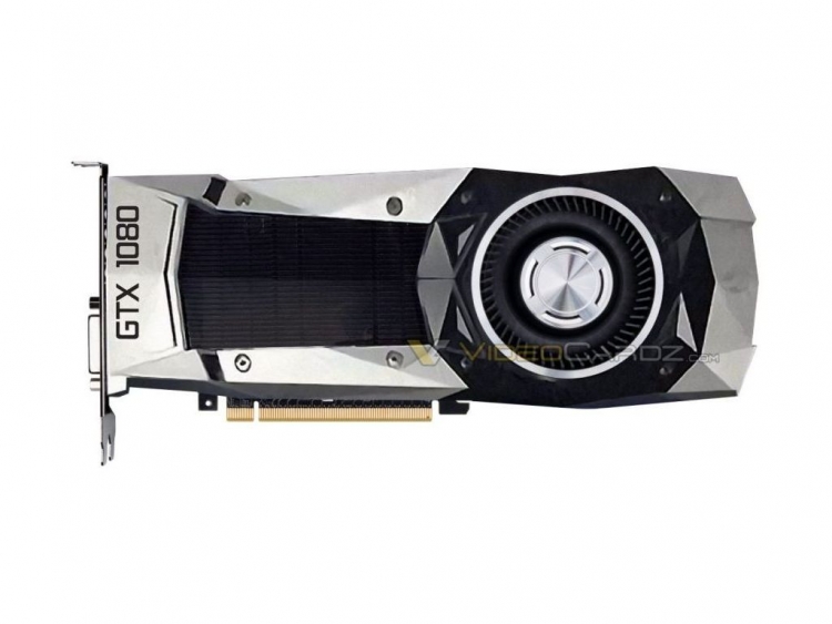
Nvidia’s Geforce GTX 1080 uses a GP104 Pascal GPU and features 2560 cores, a 1.60GHz base clock (1.73GHz boost clock) and 8GB of GDDR5X. With 9 teraflops of single-precision floating point performance, Nvidia says it will surpass the performance of two Geforce GTX 980s in SLI. The company also claims that a single Geforce GTX 1080 is faster than its current Maxwell flagship, the Geforce GTX Titan X (March 2015) based on GM200 (7 teraflops single-precision), and is just half the price.

According to the company’s own marketing slides, the card will average around 65 percent faster than a single Geforce GTX 980 and 20 to 25 percent faster than a Titan X or GTX 980 Ti. Already, the 1.60GHz base clock is a 43 percent frequency increase over a GTX 980. The card will have five display outputs – three DisplayPort 1.2 ports (1.4 “ready” with 4K at 120Hz), one HDMI 2.0b port (4K at 60Hz) and one DL-DVI port.

Another impressive note about today’s announcement was that Nvidia’s demonstration GPU during the event was overclocked from 1733MHz to a 2114MHz core speed – a modest 23 percent increase over the official boost clock. The company has confirmed that its Geforce Pascal lineup will feature vapor chamber coolers, something the 900 series did not, and this should go a long way in shaping overclocking performance results for stock cooler users.

For reference, the Geforce GTX Titan X features 3072 cores, 192 texture units, a 1GHz base clock, 12GB of GDDR5 and a 250W TDP. The current 900-series flagship, the Geforce GTX 980 Ti, features 2816 cores, 176 texture units, a 1GHz base clock, 6GB of GDDR5 and a 250W TDP.

Geforce GTX 1070 – faster than a Geforce GTX Titan Black

geforce gtx 1070 specs

The Geforce GTX 1070 uses a GP104-200 Pascal GPU and features 2048 cores, 8GB of standard GDDR5 memory and features 6.5 teraflops of single-precision floating point performance. This number effectively places the Geforce GTX 1070 right between the Geforce GTX Titan X (7 teraflops) and the Geforce GTX Titan Black (5.1 teraflops). The card will have five display outputs – three DisplayPort 1.2 ports (1.4 “ready” with 4K at 120Hz), one HDMI 2.0b port (4K at 60Hz) and one DL-DVI port.

For reference of single-precision floating point numbers, the Radeon Fury X (June 2015) achieves 8.6 teraflops, the Geforce GTX Titan Z (March 2014) gets 8.1 teraflops, the Geforce GTX Titan X (March 2015) gets 7 teraflops, the Geforce GTX 980 Ti (June 2015) gets 5.6 teraflops, and the Geforce GTX Titan Black (February 2014) gets 5.1 teraflops.

Nvidia launches new “High-Bandwidth SLI” bridges

nvidia hb sli bridge sizes

During the event, Nvidia also launched a new Scalable Link Interface (SLI) bridge for Pascal-based GPUs called “high-bandwidth SLI,” or HB SLI. The official Geforce site (towards the bottom) claims this bridge doubles the amount of available transfer bandwidth compared to running Maxwell-based GPUs in SLI.

nvidia hb sli bridges

Pricing and availability

As mentioned previously, Nvidia is glad to claim that Geforce GTX 1080 and GTX 1070 are the world’s first 16-nanometer FinFET-based GPUs. Power and performance claims aside, however, our favorite part of this launch announcement was that split second in the live stream video when some young kid in the audience gleefully yelled, “What? I can [actually] afford that!” in response to Jen-Hsun’s Geforce GTX 1080 unveiling.

nvidia geforce pascal specs

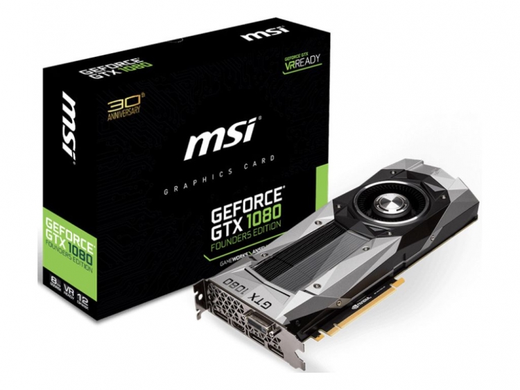
The company will launch a standard Geforce GTX 1080 for $599 along with an alternative Geforce GTX 1080 Founders Edition for $699 on Friday, May 27th.

Two weeks later on Friday, June 10th, the company will launch a standard Geforce GTX 1070 for $379 along with an alternative Geforce GTX 1070 Founders Edition for $449.

While Nvidia launched the Geforce GTX 980 in September 2014 for $50 less than the GTX 1080 and the GTX 970 for $50 less than the GTX 1070, the difference this time around is that it claims both cards are faster than the company’s current flagships – the Geforce GTX Titan X ($1000) and GTX 980 Ti ($649).


Via